Applied Materials to invest $4 bln in Silicon Valley chip research center
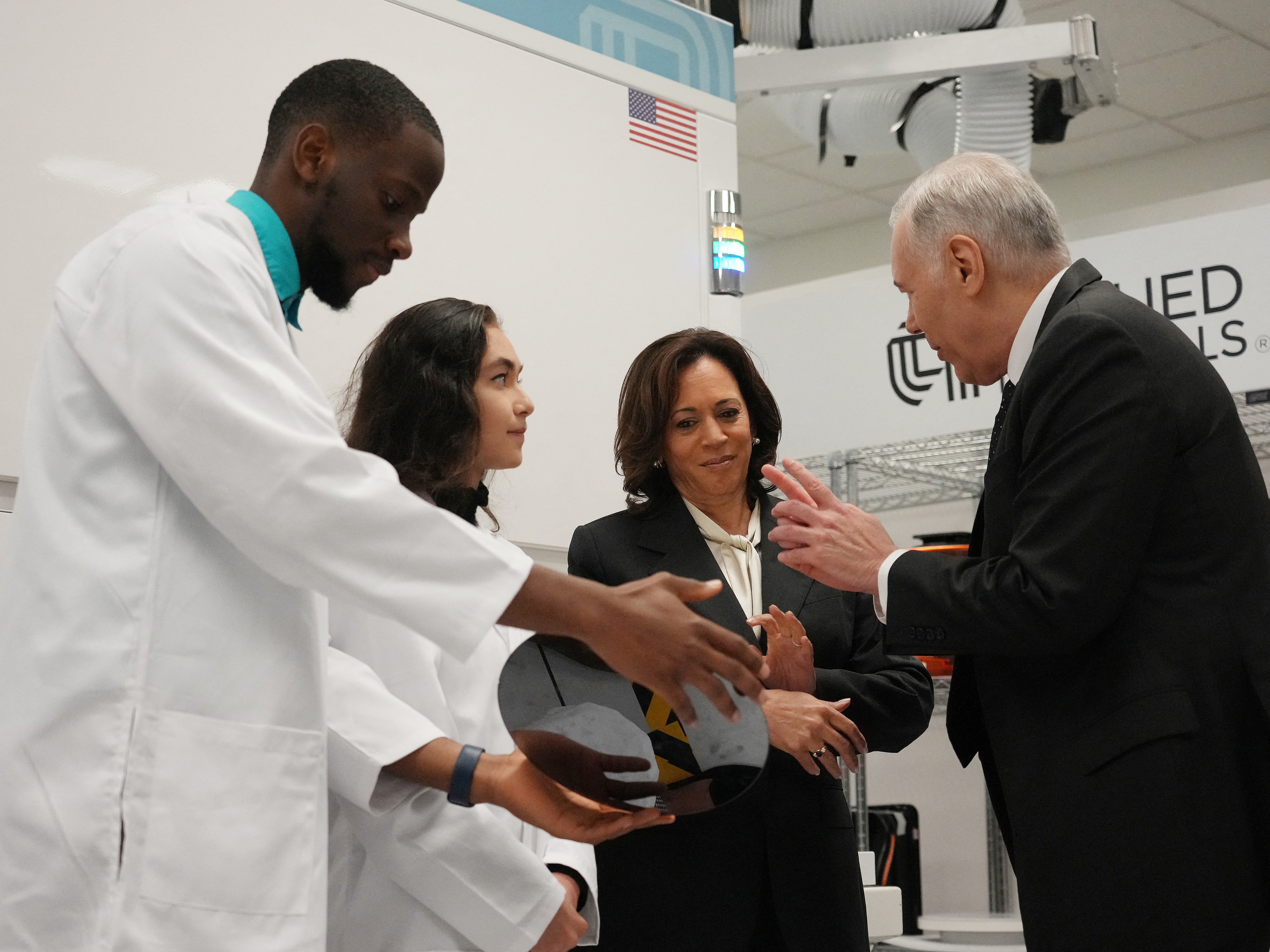
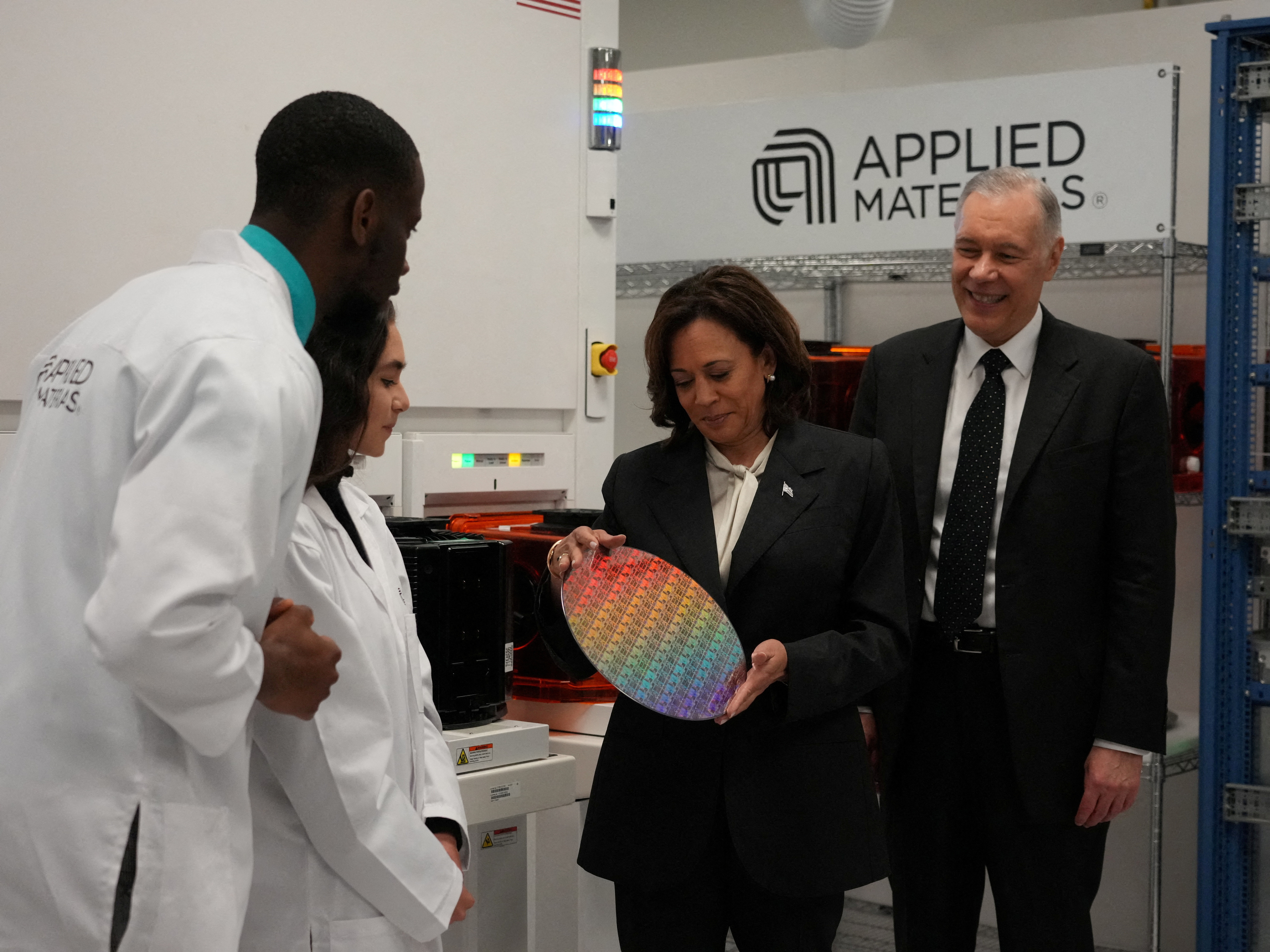
[1/3]U.S. Vice President Kamala Harris stands next to Applied Materials CEO Gary E. Dickerson and Applied Materials employees Yann Lapnet and Satomi Angelika Murayama as she tours a site where the company plans to build a research facility, in Sunnyvale, California, U.S., May 22, 2023. Jim Wilson/Pool... Purchase Licensing Rights
SANTA CLARA, California May 22 (Reuters) - U.S. semiconductor toolmaker Applied Materials Inc (AMAT.O) on Monday said it plans to spend up to $4 billion on a research center in the heart of Silicon Valley to speed up advances in semiconductor manufacturing.
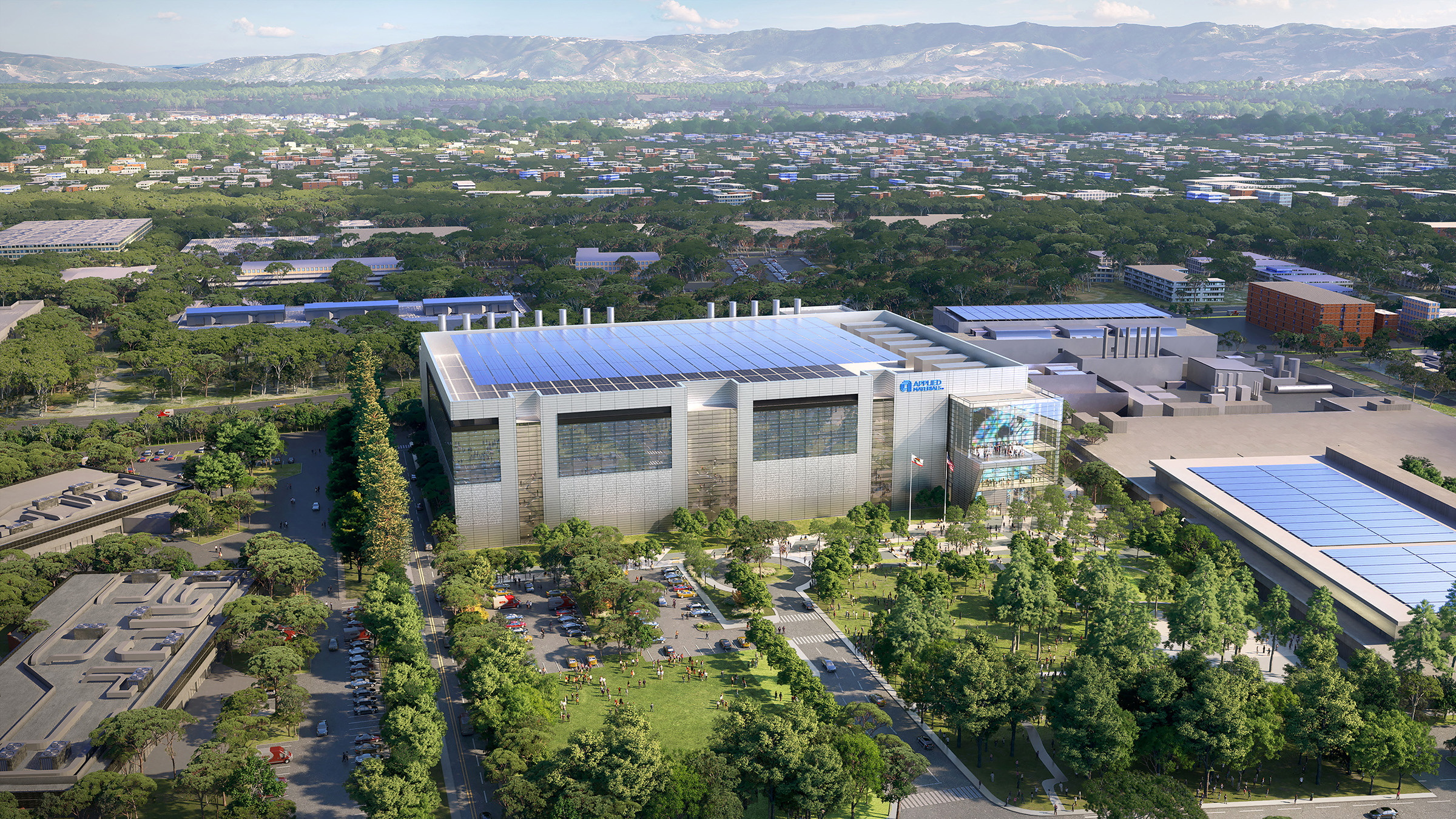
The center based in Sunnyvale, California, will come on line in 2026 and create up to 2,000 engineering jobs, said Applied, the world's biggest maker of tools used in manufacturing chips.
The facility will host about $25 billion of research work over its first decade, pulling together staff from research universities and chipmakers such as Intel Corp (INTC.O), Taiwan Semiconductor Manufacturing Co (2330.TW) and Samsung Electronics Co Ltd (005930.KS), among others.
The announcement comes as the U.S. is trying to bring back advanced semiconductor manufacturing with a $52 billion measure passed last year.
Applied Materials said the new facility, called the Equipment and Process Innovation and Commercialization (EPIC) Center, will be the size of more than three American football fields. Applied said it will invest in it over seven years and wants subsidies from the government through the CHIPS and Science Act.
"We're absolutely going to go forward. The scale of how fast we invest is going to be tied to the government incentives," Gary Dickerson, CEO of Applied Materials, told Reuters. "The economics of this are compelling in terms of accelerating the technology road maps for our customers and also for Applied."
Taking ideas from research universities and turning them into tools used in factories can take many years, said Applied executives. By putting universities and chip manufacturers under one roof with Applied, the company hopes to slash that time by nearly a third by having the three groups carry out some of their work in parallel.
U.S. Vice President Kamala Harris, who announced the news at Applied Materials' Silicon Valley event, said the investment plans were thanks to the administration's incentives.
"When completed, it will be the largest such facility in the world. And of course, it will contain some of the most cutting-edge technology," Harris said. "These investments also strengthen our national security by making sure that we have the capacity to produce semiconductors, here at home."
Senior administration officials briefing the media ahead of the event said the Commerce Department has received more than 300 statements of interest for the $39 billion portion of the CHIPS Act for manufacturing incentives. Applied Materials can apply for some of that funding, but the application requirements for such facilities will not be released until the early fall.
The CHIPS Act has another $11 billion set aside for broader R&D efforts including funding for a new National Semiconductor Technology Center that will be a focal point for the industry's research and engineering.
The Technology Roundup newsletter brings the latest news and trends straight to your inbox. Sign up here.
Reporting by Jane Lanhee Lee and Stephen Nellis in Santa Clara, California; Editing by Leslie Adler
Our Standards: The Thomson Reuters Trust Principles.